
How Flying Probe Testing Works for PCB Assembly
In this article, we will try to cover the whats, the whys, and the hows of a flying probe tester.
Historically, in-circuit testers were developed first for testing PCB assemblies; flying probe testers came later.
What is ICT or in-circuit testing?
In-circuit testing tests the workings of a PCB assembly, i.e., white box testing. Here, we use electric probes to check the populated PCB for shorts, opens, and values of resistance, capacitance, and other basic qualities. Traditionally, ICT utilized a “bed of nails” fixture based method of testing. For every PCB assembly, it is required to have a custom ICT fixture comprising of a set of spring-loaded pogo pins that contact the PCBA at the locations of the designed test points. Each pogo pin connects with one node/test point in the PCBA under test.
The custom ICT fixture required for a new PCBA assembly can be awfully expensive, especially for a complex PCBA. And it may take a few days to manufacture an ICT fixture, this method of testing is only suitable for testing large volumes of production; it is neither cost-effective nor time-effective for smaller lots or prototype lots of production.
What is flying probe test?
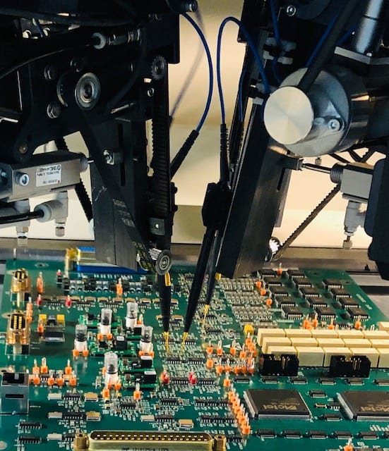
The Flying Probe Tester in our PCB assembly facility
Flying probe testing, as the name implies uses test probes that “fly” i.e. the test probes move from test points to other test points as per instructions given by the specific software program that is written for the board under test. No custom fixture is required, so it could also be called as fixtureless in-circuit test if used on an assembled PCB. Hence, it is highly cost-effective for prototypes and low to mid-volume production.
The flying probe testers originally evolved for use only for bare board testing, and they have become the de-facto standard for bare-boards testing (which involves testing for shorts, opens, etc. between copper conductor features on the bare PCB) where the main electrical parameter that is measured is the resistance between two points or nodes.
However, slowly FPTs evolved to measure even the capacitance and inductance in addition to mere resistance. This made them beneficial for use on PCB assemblies as well. Not only this, but there are also several reasons for their eventual adoption for testing of the populated boards:
- Firstly, as mentioned earlier, they are more cost-effective for smaller lots of production.
- Secondly, they do not pose as many accessibility issues as is the case for ICT testers using pogo pins; the FPT probes points are smaller as compared to pogo pins, and they are able to access much smaller pads than test points for pogo pins. For ICT testing, the test points have been designed specifically while this is rarely required for FPT testing.
- Thirdly, as the movement of probes in an FPT is controlled by a software program that is easy to change, flexible testing strategies are easy to implement. Furthermore, it is also much easier to adjust probe landing position changes through software change.
- Fourthly, since flying probes can access component pins directly through automated probing, requiring no specifically built test points, it provides an improved test coverage over traditional ICT testing.
The FPTs are equipped with a camera to inspect component polarity. They have now become a more attractive method of testing, especially with the ongoing miniaturization trend in electronics. Why is it so? For our smaller size electronic gadgets, board real estate can be a very precious commodity, and thus elimination of some, if not all, test points are very helpful in their PCB design.
For reasons stated earlier, flying probe testing has now become a preferred and cost-effective method for testing low-volume and prototype circuit boards. It’s easy to program and use even for very dense and complex boards.
Furthermore, there are great advances taking place in the technology of the FPT field, mainly in the effort to increase the test coverage percentage, and thereby increasing the quality and reducing the time of testing. Thus, FPT has great potential to decrease the product design cycle and reducing time to market.
How flying probe testing works?
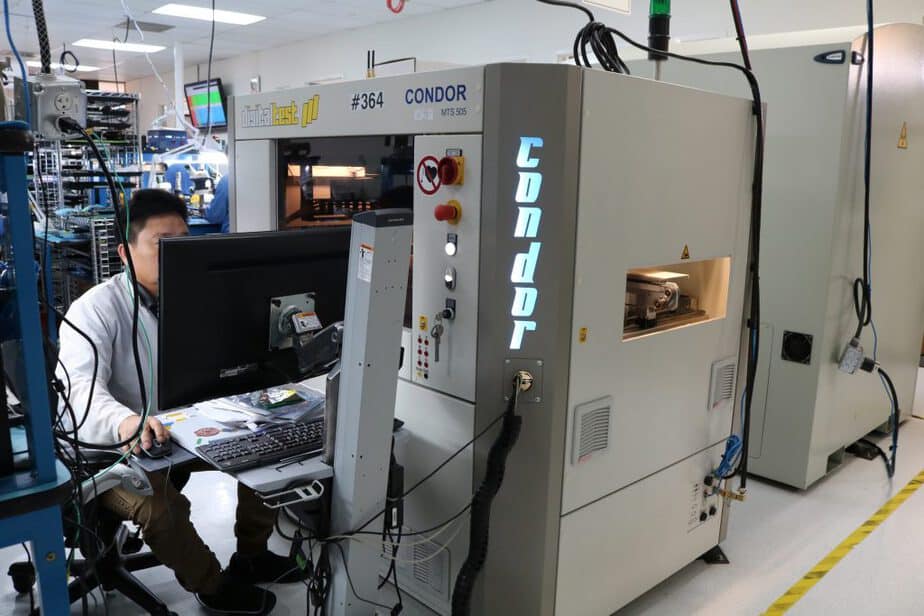
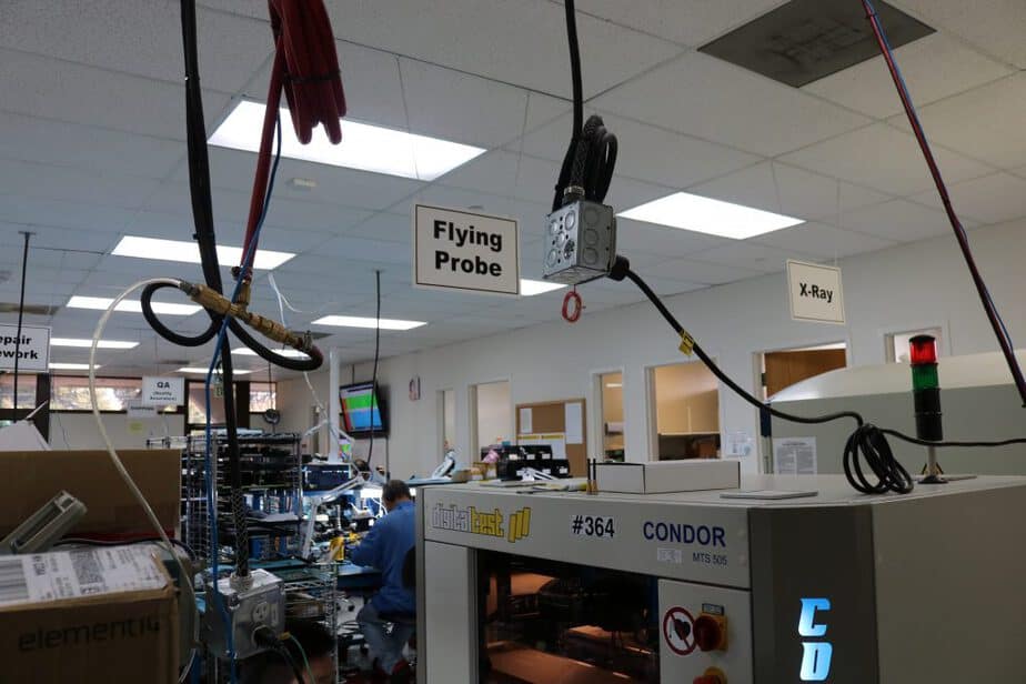
Our expert working on the tester software
Here, we will discuss briefly the process of flying probe testing.
In order to be able to test a circuit board assembly in the FPT, we need to create an FPT test program. This program is generally created offline on a PC (just like an SMT program for a pick-and-place machine is created offline on a PC using an SMT programming application).
This is how it is created:
Every FPT provides a Test Program Generating Application that runs on a PC. This application requires the PCB assembly’s BOM and the ECAD file. The Gerbers alone are not sufficient for this; the ECAD file needs to be an intelligent CAD file, which means that it should be either in ODB++ format or IPC-2581 format or native ECAD design file format as per the ECAD software tool (e.g. Allegro or Altium or PADS etc.) that was used in designing the PCB. The BOM needs to be in an EXCEL format.
Once the test program is generated, it is loaded into the FPT tester. The circuit board assembly to be tested, which could be either a single board or an array of boards, is put on a conveyer belt so that it can travel inside the tester area where the probes are.
When the test program is run, the probes, under the control of the test program, will contact the pads (component pads and test pads if any) and the unmasked vias as per the test program already loaded into the tester, and tester will apply electrical test signals and power to the probe points and make measurements thereof.
These measurements will be processed inside the tester and to find if the circuit portion within the probes is giving expected results (as per components there) within already specified tolerances. In this manner, FPT detects the defects of that unit. FPT hardware is equipped with signal generators, dc and ac power supplies, various types of sensors, a multiplexing system, digital multimeters, frequency counters, etc. which are used to provide signals with which to excite the PCB nodes and to make measurements on the nodes of the components and interconnections on the PCB assembly.
By a complex scheme of excitation signals, FPT tries to isolate, as far as feasible, the component segments between the testing probes from the rest of the interconnections to other components on the board. This “virtual isolation” of components from the rest of the circuit interconnections makes it possible to measure component values as accurately as feasible, while they still remain connected in the circuitry on the board.
As stated earlier, the flying probe tester can test for shorts, opens, and component values. An FPT is also equipped with a camera to help in inspecting component polarity automatically. It also performs “diode” impedance tests on inputs of integrated devices whose functional behavior is outside the scope of testing of the FPT. Add to this, most FPTs in the market today are also able to excite with signals and make some measurements on those pads of the ICs which are underneath their bodies (like BGAs, QFNs, and other leadless devices) by way of capacitive probing!
In short, an FPT tries to test the board as comprehensively as possible given the accessibility constraints of a given board design.
Let us now mention some emerging advanced features about testing through the probes:
Phase difference measurement unit
The phase difference measurement unit – PDM – sends a high-frequency signal between the reference line and signal line’s sections’ one endpoint, and measures the phase of the signal at the other endpoint – thus estimating their phase difference. This should cut down isolation tests within a net.
High Voltage Stress Test (HVS)
The high voltage stress test is for the high resistance undetected isolation defects by PDM. We conduct HVS by applying high voltage pulses between signal lines to detect high resistance defects. HVS and PDM are similar in the aspect that both inspect each net once. Thus, is rapid on time.
How high is high? While the maximum applicable voltage with standard isolation resistance measurement is usually 250V, HVS offers the option of applying about 500V to 1000V, while ensuring that HVS uses a low power test, so that a super high resistance test is conducted without adding high stress on the tested boards.
Micro shorts detection
Next on our platter is micro-short detection. The sudden application of a high voltage in isolation tests may cause burning out of parts containing micro shorts. Micro-short tests can avoid such damage and trouble by applying a low voltage before gradually increasing the applying voltage. Sometimes, high resistance short between multiple layers of a board possesses the characteristics of semiconductors and capacitors. The reversing of the polarity of high voltagecould also detect these defects.


1 Comments
https://usa.pcbpower.com/blog/flying-probe-test-and-benefits-for-pcbs?utm_source=https%3A%2F%2Fusa.pcbpower.com%2Fblog%2Fflying-probe-test-and-benefits-for-pcbs&utm_medium=Modi+Kushal&utm_id=Modi+Kushal
ReplyDeleteLeave a Reply
Your email address will not be published. Required fields are marked*
Comment